


5 Tricks About Electron Beam Lithography You Wish You Knew Before
Electron Beam Lithography technology refers to a lithographic method for direct writing which employs a focused electron beam for the forming of models by modifying material, deposition of materials (additives), or removing materials (subtractive). As a result of its high resolution, simplicity, and lack of masking requirements, electron beam lithography is a popular production process in the semiconductor industry. Electronics have sufficient energy to cause a chemical or structural surface modification in the material modification mode, electrons are used in material deposition to induce a surface deposition of a volatile compound and the e-beam is energetic enough to take off parts of the material from a substratum in removal mode. Electron lithography gives greater levels, in opposition to photon-based photography.
The lithography system for electrons is used to scan a concentrated electron beam and create unique forms on electron-sensitive-resistant surfaces. In application areas where the writing of micro-and nanostructures on a wide range of materials occurs, Electron Beam Lithography (EBL) or EBeam Technology remains a preferred device. In the national labs, research universities, and other sectors there are several examples of routine usage. Note that nanoscale size structures on areas up to mm2 are written on the current EBL machine.
Ideally, a relatively basic idea is implemented in the electron beam lithography system. Somehow photolithography is comparable to the EBL lithography concept of work. Thus a concentrated electron beam is scanned through the substratum of an electron-sensitive substance called resistance. The resistance alters its solubility characteristics by the energy the electron beam deposits. Through development, the regions exposed to the resistance tone will be eliminated.
Now you may ask that there is an additive called EMB which stands for Electron Beam Melting. The Electron Beam Melting (EBM) process is a high-powered electron beam that is used to produce the energy required for melting and high productivity in lithography. In addition, the vacuum maintains a clean and regulated atmosphere. Through fewer supports, Electron beam melting technology allows for greater design freedom. Thanks to densely stacked parts, it also allows for larger volume production. Complex and detailed manufactured products using this combination.
Electronic beam lithography (EBL) is a slower form of patterning than photolithography or stamping. Cleanroom amenities are required. Photomasks are time-consuming and inefficient, thus electron beam lithography is better suited to high-resolution patterns or unique objects.
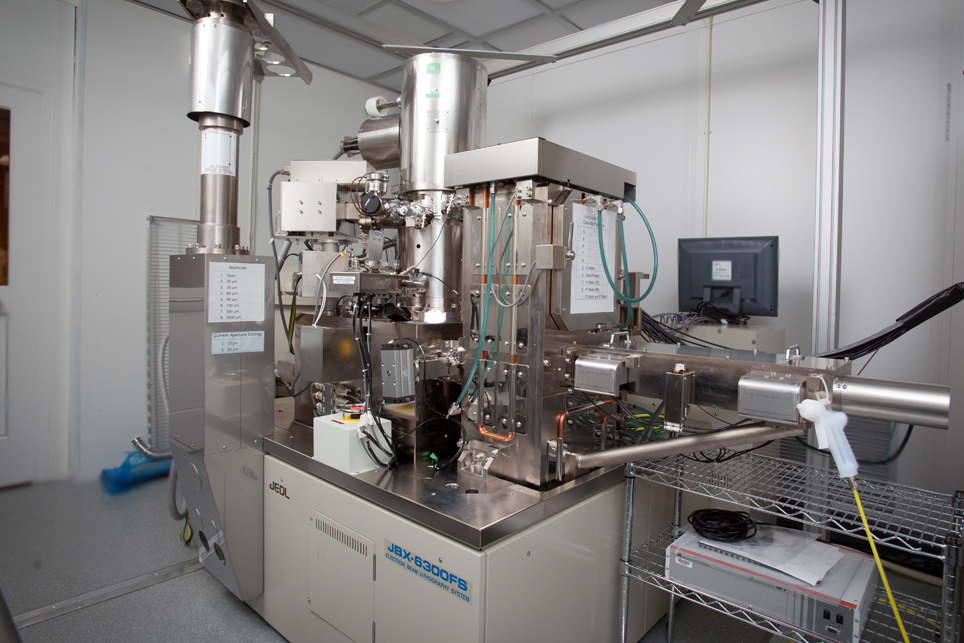
The EBL system consists of numerous components. The components include:
- The electron gun or source of electron
- A column designing and concentrating the electron beam
- A mechanical stage for placing the wafer under the beam
- The wafer handling system for wafer feeding and unloading after processing Computer – control system for other components automated.
- Computer control system.
In the following, we describe the best 5 tricks that can be optimized for Electron Beam Lithography.
Table of Contents
Acceleration Voltage Determination
With the acceleration voltage, the clearance dosage of a resistor rises. This is due to the fact that the forward-scattering electrons will transfer more energy efficiency to the resistor at lower acceleration voltages (total of 10 kV), leading to lower clearing levels, but at the cost of increasing beam spot and increased line roughness.
Choose the Aperture Size of the Collimation
With replaceable openings in the strap, the electron beam may be collimated and current-limited. It is found that the only parameter that may lower the overall writing time directly is the beam current for a certain pattern and resist with a certain sensitivity.
Enabling High Current Mode
Raith is called a “high current” mode, where the focusing properties of the condenser lens are changed, resulting in an overall narrower, parallel beam. Its critical size is restricted by electron scattering, which occurs in both the electron beam resists and the substrates used. EBL systems with high acceleration voltages are required to produce precise patterns. Smaller scattering angles in the resist and a broad secondary-electron spread in the substrates are the main advantages of these resists.
Write-Field Size
A typical write-field size is 100 μm × 100 μm. You can select a large write-field of 1000 μm × 1000 μm (where the largest available is 2000 μm × 2000 μm), resulting in the pattern being reproduced from a 100 times fewer write-fields.
Write Mode
There are usually two ways to move the beam inside one typeface: a vector scan and a raster scan. The raster scan is a simpler, but often time-consuming technique. The beam is swept throughout the whole writing field in a raster scan and blank when passing across regions to be exposed. The more technically difficult vector scan moves the beam straight to each exposed region and only scans the areas. We see that the saving time by utilizing a vector scan is significantly dependent on the model type to be created. A very regular pattern can even be produced more quickly utilizing a raster scan method, with numerous tiny, open, and closed regions.